- 您现在的位置:买卖IC网 > Sheet目录3753 > ATMEGA169P-16MCHR (Atmel)MCU AVR 16KB FLASH 16MHZ 64-VQFN
PIC16F946
DS41265A-page 238
Preliminary
2005 Microchip Technology Inc.
19.5
Timing Parameter Symbology
The timing parameter symbols have been created with
one of the following formats:
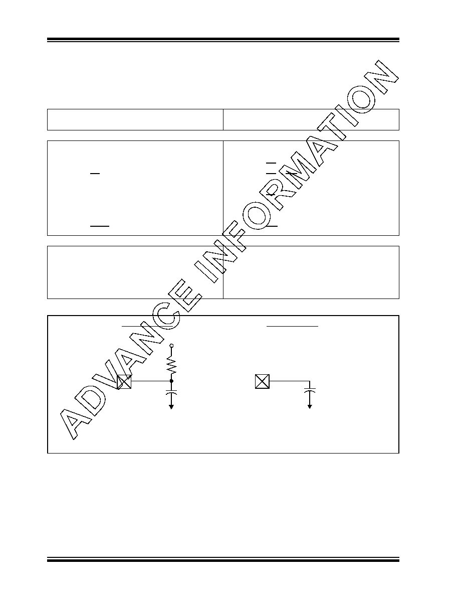
FIGURE 19-2:
LOAD CONDITIONS
1. TppS2ppS
2. TppS
T
F
Frequency
T
Time
Lowercase letters (pp) and their meanings:
pp
cc
CCP1
osc
OSC1
ck
CLKO
rd
RD
cs
CS
rw
RD or WR
di
SDI
sc
SCK
do
SDO
ss
SS
dt
Data in
t0
T0CKI
io
I/O port
t1
T1CKI
mc
MCLR
wr
WR
Uppercase letters and their meanings:
S
FFall
P
Period
HHigh
R
Rise
I
Invalid (High-impedance)
V
Valid
L
Low
Z
High-impedance
VDD/2
CL
RL
PIN
VSS
CL
RL = 464
Ω
CL = 50 pF for all pins
15 pF for OSC2 output
Load Condition 1
Load Condition 2
Legend:
发布紧急采购,3分钟左右您将得到回复。
相关PDF资料
2-1546217-0
TERM BLK RCPT 20POS SIDE 5.08MM
1-1546217-9
TERM BLK RCPT 19POS SIDE 5.08MM
1-1546217-8
TERM BLK RCPT 18POS SIDE 5.08MM
1-1546217-7
TERM BLK RCPT 17POS SIDE 5.08MM
1-1546217-6
TERM BLK RCPT 16POS SIDE 5.08MM
1-1546217-5
TERM BLK RCPT 15POS SIDE 5.08MM
1-1546217-4
TERM BLK RCPT 14POS SIDE 5.08MM
1-1546217-3
TERM BLK RCPT 13POS SIDE 5.08MM
相关代理商/技术参数
ATMEGA169P-16MCU
功能描述:8位微控制器 -MCU AVR 16KB, 512B EE 16MHz 1KB SRAM, 5V
RoHS:否 制造商:Silicon Labs 核心:8051 处理器系列:C8051F39x 数据总线宽度:8 bit 最大时钟频率:50 MHz 程序存储器大小:16 KB 数据 RAM 大小:1 KB 片上 ADC:Yes 工作电源电压:1.8 V to 3.6 V 工作温度范围:- 40 C to + 105 C 封装 / 箱体:QFN-20 安装风格:SMD/SMT
ATMEGA169P-16MU
功能描述:8位微控制器 -MCU AVR 16K FLASH 512B EE 1K SRAM LCD ADC RoHS:否 制造商:Silicon Labs 核心:8051 处理器系列:C8051F39x 数据总线宽度:8 bit 最大时钟频率:50 MHz 程序存储器大小:16 KB 数据 RAM 大小:1 KB 片上 ADC:Yes 工作电源电压:1.8 V to 3.6 V 工作温度范围:- 40 C to + 105 C 封装 / 箱体:QFN-20 安装风格:SMD/SMT
ATMEGA169P-16MU SL383
制造商:Atmel Corporation 功能描述:MCU 8BIT ATMEGA RISC 16KB FLASH 3.3V/5V 64PIN MLF - Tape and Reel
ATMEGA169P-16MUR
功能描述:8位微控制器 -MCU AVR LCD 16KB FLSH EE 512B 1KB SRAM-16MHZ RoHS:否 制造商:Silicon Labs 核心:8051 处理器系列:C8051F39x 数据总线宽度:8 bit 最大时钟频率:50 MHz 程序存储器大小:16 KB 数据 RAM 大小:1 KB 片上 ADC:Yes 工作电源电压:1.8 V to 3.6 V 工作温度范围:- 40 C to + 105 C 封装 / 箱体:QFN-20 安装风格:SMD/SMT
ATMEGA169P-8AU
制造商:ATMEL 制造商全称:ATMEL Corporation 功能描述:Microcontroller with 16K Bytes In-System Programmable Flash
ATMEGA169P-8MU
制造商:ATMEL 制造商全称:ATMEL Corporation 功能描述:Microcontroller with 16K Bytes In-System Programmable Flash
ATMEGA169PA
制造商:ATMEL 制造商全称:ATMEL Corporation 功能描述:8-bit Microcontroller with 16K Bytes In-System Programmable Flash
ATMEGA169PA_1
制造商:ATMEL 制造商全称:ATMEL Corporation 功能描述:High Endurance Non-volatile Memory segments